(Hong Kong)

Product Summary
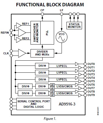
The AD9516-3BCPZ clock generator provides a multi-output clock distribution function with subpicosecond jitter performance, along with an on-chip PLL and VCO. The on-chip VCO tunes from 1.75 GHz to 2.25 GHz. Optionally, an external VCO/VCXO of up to 2.4 GHz can be used. The AD9516-3BCPZ emphasizes low jitter and phase noise to maximize data converter performance, and it can benefit other applications with demanding phase noise and jitter requirements. The AD9516-3BCPZ features six LVPECL outputs (in three pairs) and four LVDS outputs (in two pairs). Each LVDS output can be reconfigured as two CMOS outputs. The LVPECL outputs operate to 1.6 GHz, the LVDS outputs operate to 800 MHz, and the CMOS outputs operate to 250 MHz.
Parametrics
AD9516-3BCPZ absolute maximum ratings: (1)VS, VS_LVPECL to GND: -0.3 V to +3.6 V; (2)VCP to GND: -0.3 V to+5.8 V; (3)REFIN, REFIN to GND: -0.3 V to VS + 0.3 V; (4)REFIN to REFIN: -3.3 V to +3.3 V; (5)RSET to GND: -0.3 V to VS + 0.3 V; (6)CPRSET to GND: -0.3 V to VS + 0.3 V; (7)CLK, CLK to GND: -0.3 V to VS + 0.3 V; (8)CLK to CLK: -1.2 V to +1.2 V; (9)SCLK, SDIO, SDO, CS to GND: -0.3 V to VS + 0.3 V; (10)OUT0, OUT0, OUT1, OUT1, OUT2, OUT2, OUT3, OUT3, OUT4, OUT4, OUT5, OUT5, OUT6, OUT6, OUT7, OUT7, OUT8, OUT8, OUT9, OUT9 to GND: -0.3 V to VS + 0.3 V; (11)SYNC to GND: -0.3 V to VS + 0.3 V; (12)REFMON, STATUS, LD to GND: -0.3 V to VS + 0.3 V; (13)Junction Temperature: 150℃; (14)Storage Temperature Range: -65℃ to +150℃; (15)Lead Temperature (10 sec): 300℃.
Features
AD9516-3BCPZ features: (1)Low phase noise, phase-locked loop (PLL); (2)On-chip VCO tunes from 1.75 GHz to 2.25 GHz; (3)External VCO/VCXO to 2.4 GHz optional; (4)1 differential or 2 single-ended reference inputs; (5)Reference monitoring capability; (6)Automatic revertive and manual reference switchover/holdover modes; (7)Accepts LVPECL, LVDS, or CMOS references to 250 MHz; (8)Programmable delays in path to PFD; (9)Digital or analog lock detect, selectable; (10)6 pairs of 1.6 GHz LVPECL outputs; (11)Each output pair shares a 1-to-32 divider with coarse phase delay; (12)Additive output jitter: 225 fs rms; (13)Channel-to-channel skew paired outputs of <10 ps; (14)4 pairs of 800 MHz LVDS clock outputs; (15)Each output pair shares two cascaded 1-to-32 dividers with coarse phase delay; (16)Additive output jitter: 275 fs rms; (17)Fine delay adjust (Δt) on each LVDS output; (18)Each LVDS output can be reconfigured as two 250 MHz CMOS outputs; (19)Automatic synchronization of all outputs on power-up; (20)Manual output synchronization available; (21)64-lead LFCSP.
Diagrams
| Image | Part No | Mfg | Description |  |
Pricing (USD) |
Quantity | ||||||||||||||||
|---|---|---|---|---|---|---|---|---|---|---|---|---|---|---|---|---|---|---|---|---|---|---|
 |
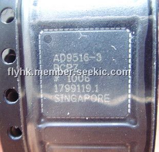
 AD9516-3BCPZ |
|
IC CLOCK PLL/VCO 2GHZ 64LFCSP |
Data Sheet |
|
|
||||||||||||||||
|
AD9516-3BCPZ-REEL7 |
|
IC CLOCK PLL/VCO 2GHZ 64LFCSP |
Data Sheet |
|
|
||||||||||||||||